

 Company expands production of organic packages for microelectronic devices used in smartphones and tablet PCs
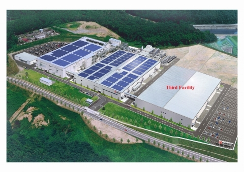
Kyocera Corporation (NYSE:KYO)(TOKYO:6971) today announced that it will begin construction this week on a third manufacturing facility at its Kyoto Ayabe complex in Ayabe City, Kyoto Pref., Japan. The new facility will produce miniaturized, low-profile organic packages to house microelectronic devices used inside smartphones, tablet PCs and related mobile communications equipment.
Kyocera’s microelectronic packaging technology can facilitate higher functionality, greater integration and slimmer designs in mobile communications equipment. The market for Kyocera’s package products is expected to grow as consumer devices incorporate multiple internal modules for camera, wireless, power amplifier and control functions.
In addition, the expanding IoT (Internet of Things) trend is expected to generate new applications for Kyocera products as wireless chips and sensor chips are increasingly modularized into packaging solutions based on organic material technology.
Until April 1, 2016, the Kyoto Ayabe complex was operated by the former Kyocera Circuit Solutions, Inc. (“KCS”), Kyocera’s wholly owned subsidiary specializing in high-density organic wiring boards, packages and large-scale printed motherboards for semiconductor devices. On April 1, 2016, KCS was merged into Kyocera Corporation as part of a business integration strategy to enhance the development of new products and markets while further expanding business synergies.
Since 2005, Kyocera’s Kyoto Ayabe complex has manufactured a wide range of organic packaging products, including FC-BGA (flip-chip ball grid array) substrates for high-end application-specific integrated circuits (ASICs). Over the years, Kyocera has cultivated cutting-edge technologies in high-density wiring and automated production processes to create smaller, lower-profile products. Kyocera’s second facility at Kyoto Ayabe was added in the summer of 2014, and the third, targeted for completion in December 2016, will strategically expand the company’s capabilities.
Outline of the Third Facility
Name Kyoto Ayabe Plant, Third Facility
Location Ayabe City, Kyoto Pref., Japan
Facility size Building area: 13,143m2 (steel-framed, two floors, 140×84m)
Floor space: 25,420m2
Construction plan Groundbreaking: April 21, 2016 (planned)
Completion: December 2016 (planned)
Start of operations April 2017 (planned)
Production Organic packages for telecommunication devices
Note: The factory building will be designed with environmental consideration such as reuse of water emissions.
www.kyocera.com

